Verification of Charge Transfer in Metal-Insulator-Oxide Semiconductor Diodes via Defect Engineering of Insulator

Verification of Charge Transfer in Metal-Insulator-Oxide Semiconductor Diodes via Defect Engineering of Insulator

Filamentary Resistive Switching and Capacitance-Voltage Characteristics of the a-IGZO/TiO2 Memory. - Abstract - Europe PMC

I-V characteristics of TiON films prepared via (a) single-step and (b)

Figure 3 from Charge Trapping Memory Characteristics of Amorphous-Indium–Gallium–Zinc Oxide Thin-Film Transistors With Defect-Engineered Alumina Dielectric

Limitations of Mott-Schottky Analysis for Organic Metal-Insulator-Semiconductor Capacitors

Ion-gating analysis on conduction mechanisms in oxide semiconductors - ScienceDirect

Role of defects on the transparent conducting properties of binary metal oxide thin film electrodes - ScienceDirect
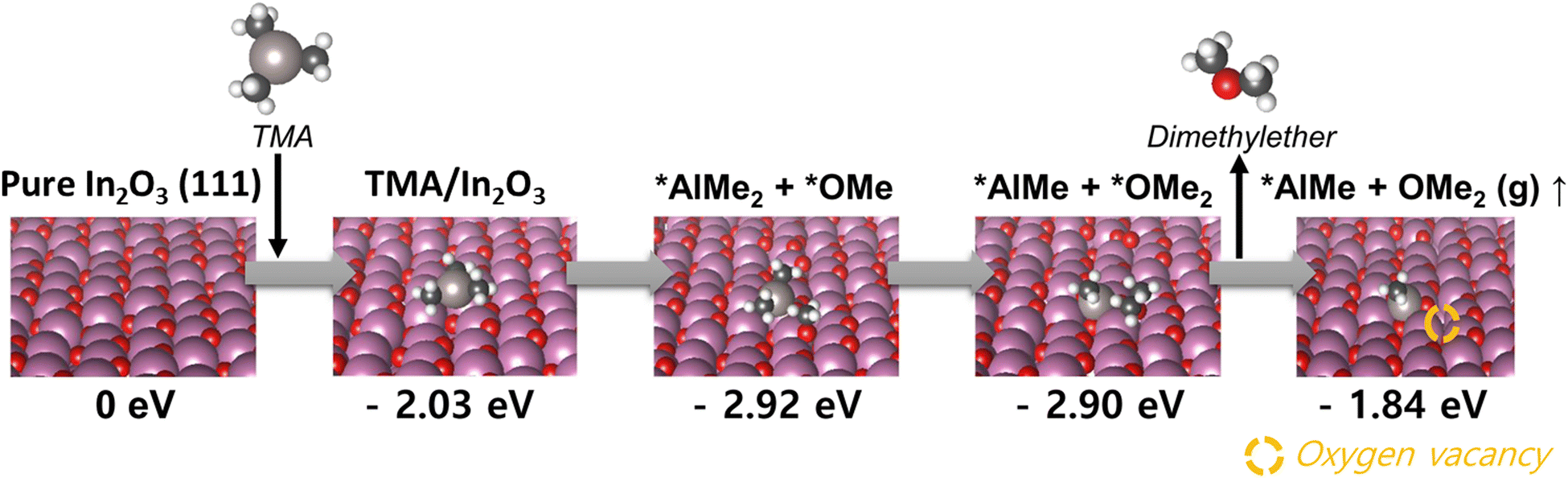
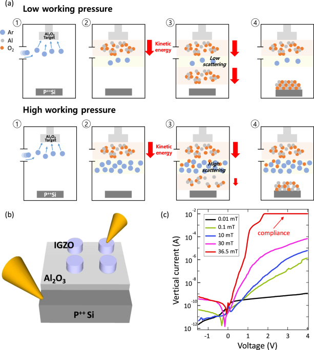
High-performance oxide thin-film diode and its conduction mechanism based on ALD-assisted interface engineering - Journal of Materials Chemistry C (RSC Publishing) DOI:10.1039/D2TC03751C

Materials, Free Full-Text

Gate and drain current behavior with variation of structural parameters
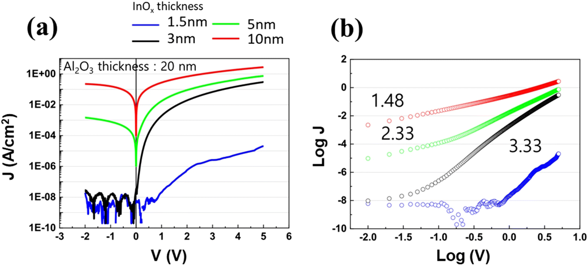
High-performance oxide thin-film diode and its conduction mechanism based on ALD-assisted interface engineering - Journal of Materials Chemistry C (RSC Publishing) DOI:10.1039/D2TC03751C

On Practical Charge Injection at the Metal/Organic Semiconductor Interface

Figure 3 from Charge Trapping Memory Characteristics of Amorphous-Indium–Gallium–Zinc Oxide Thin-Film Transistors With Defect-Engineered Alumina Dielectric

Effect of the electron mobility of the top semiconductor electrode on

On Practical Charge Injection at the Metal/Organic Semiconductor Interface