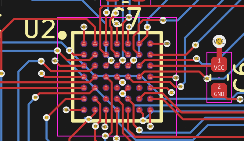
Details of test chip designs: pad pitch, layout, materials, and


Details of test chip designs: pad pitch, layout, materials, and

Changqing LIU, Loughborough University, Loughborough

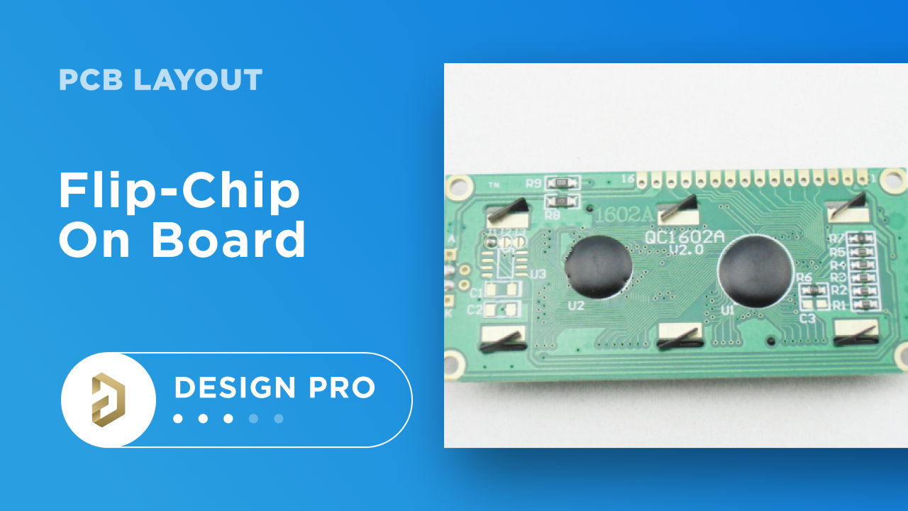
RDL and Flip Chip Design

David WHALLEY, Visiting Fellow, B.Sc. M.Phil.

Changqing LIU, Loughborough University, Loughborough

How To Design A BGA, PDF, Printed Circuit Board
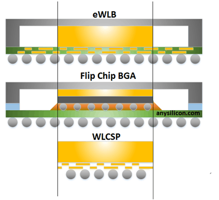
Understanding Wafer Bumping Packaging Technology - AnySilicon

Multiple System and Heterogeneous Integration with TSV-Interposers

Details of test chip designs: pad pitch, layout, materials, and opening.
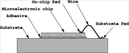
PCB Design Rules for Chip-on-Board Layout

David WHALLEY, Visiting Fellow, B.Sc. M.Phil.
Chip Design Made Easy - Wikibooks, open books for an open world
Working With BGAs: Design And Layout
Top PCB Layout Recommendations for BGA Packages


Related products